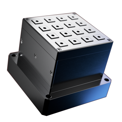
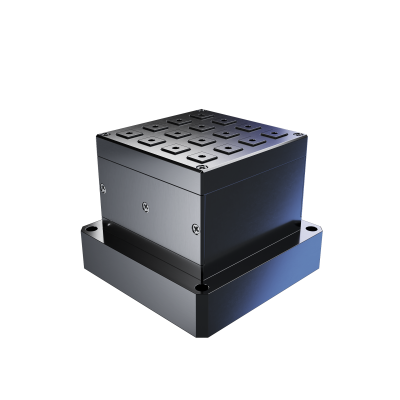
“We have created a hybrid solution with smart actuator arrays to cover the customer requirements of tomorrow.”
Engineers Jonas Reiser and Mathias Winter give insights into the development process of PI's surface shaping solutions for the future.
Driving Markets & Applications
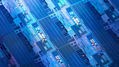
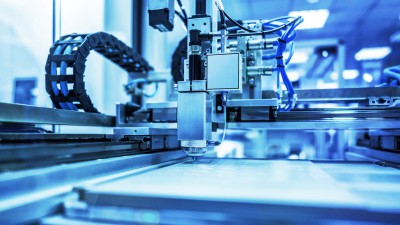
Shaping surfaces of optical components or substrates with high resolution will make it possible to increase imaging and manufacturing quality, e.g. in laser processing applications or in the highly sensitive semiconductor production.


Contact Us!
We look forward to your projects and challenges to push the limits of what is technically possible together with you.
